Last Combinatorial Screening of perovskite composition via sublimation
Solvent free preparation of perovskite films is advantageous, as no harmful solvents are needed and it is easy to control the film thickness. Multiple source sublimation of perovskite precursors is the method that is used extensively in this project, however, not all perovskite precursors have a constant sublimation behaviour which is needed to reproducibly prepare the perovskites. This limits the design freedom of the perovskite composition as only a certain number of precursors lead to reproducible perovskite films. Therefore, the first achievement in HELD has been the development of a sublimation method that allows for a much wider range of perovskite precursors to be used. With this achievement, we are able to expand the type of perovskite compositions that can be deposited into thin films. Now that more perovskite precursors are accessible for use in multiple source sublimation it is important to have a method that enables a fast screening of the perovskite thin film properties. For this we have developed a combinatorial approach to perovskite film growth, such that in a single sublimation run, a wide range of perovskite compositions are obtained depending on the substrate position with respect to the sublimation sources.
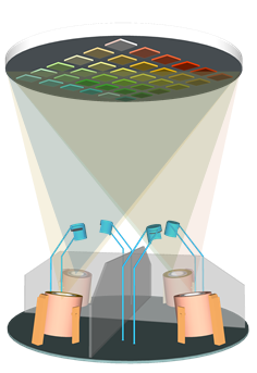
Schematic of the combinatorial approach to rapidly evaluate perovskite compositions in thin films
First perovskite-organic semiconductor heterostructures
Using sequential vacuum deposition, we were able to prepare heterostructures consisting of repeating perovskite-organic semiconductor stacks. In these structures amplified spontaneous emission was observed under optical excitation, which is a first important step towards the goal of lasing devices.
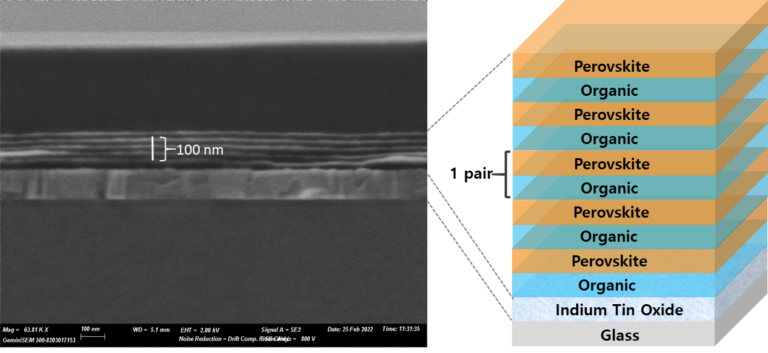
SEM cross-section image and sketch of a perovskite-organic semiconductor heterostructure
Soft deposition of transparent conductors using pulsed laser deposition
Solar cells and LEDs need at least one transparent electrode to allow light to enter and escape from the device, respectively. Our very thin film (< 1 micrometer) devices need a substrate on which the active layers are deposited. Most devices employ a transparent substrate such as glass or a plastic foil that contains a transparent conductive oxide. These devices were then finished by vacuum depositing a thin metal electrode on top of the active layers. This configuration has some limitations, especially if driving electronics needs to be integrated, for example when the LEDs are used in display applications. Another configuration in which the transparent electrode is deposited on top of the active layers, is thus often preferred to maximize performance and device integration. In HELD, the semiconductor films are very thin (< 1 µm), which makes it difficult to deposit the most transparent conducting materials without damaging the underlying films and/or generating short-circuits with the bottom electrode. Using an industrial pulsed laser deposition (PLD) tool from SOLMATES BV, we have developed a method enabling us to directly deposit transparent conductive oxides on perovskite films without damaging the active layers. This will greatly enhance our capability to integrate the novel semiconductors in the targeted applications
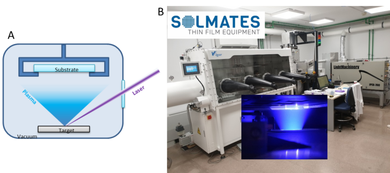
Pulsed Laser Deposition. A. schematic of its functioning, a high energy laser pulse hits the target of the material to be deposited, which then forms a plasma and reaches the substrate above it. B Image of the tool, inset shows the plasma formed after the laser pulse hits the indium tin oxide target.
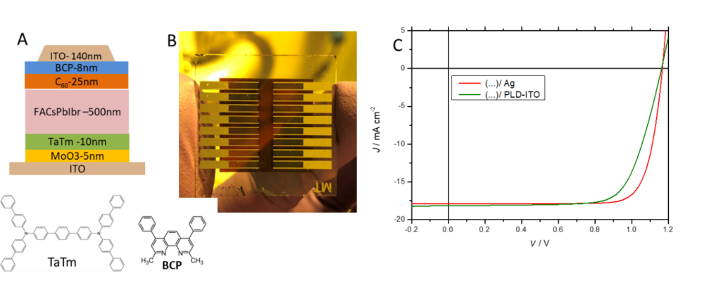
Bifacial-perovskite based solar cells where the top transparent electrode (ITO) was deposited by PLD. A: Schematic of the device architecture and the chemical structures of the used organic semiconductors. B: Image of our test substrate with 16 individual pixels. C: current density versus voltage characteristics of the cells under simulated sunlight (AM 1.5) and compared with a reference device employing a metallic Ag top electrode.
Large area perovskite solar cells in the substrate configuration deposited on a metal coated substrate and with a transparent top electrode deposited by PLD.
Thin film passivation using atomic layer depositon
In this first period we have focussed on the integration of the perovskite films in photovoltaic and light-emitting devices. Essential for applications but also for device characterization is an efficient encapsulation method that is compatible with the sensitive materials constituting the device. We developed a low temperature atomic layer deposition method by which we seal the whole device with a layer of aluminum oxide that completely eliminates the interaction with water and oxygen from the air.
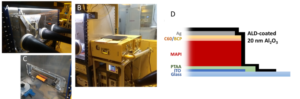
Atomic Layer Deposition Encapsulation method. A. Image of the inert glovebox used to insert the samples. B. Image of our ALD tool. C. Image of the sample introduction port. D. Schematic of a encapsulated solar cell.
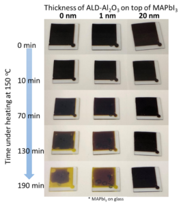
Thanks to this sealing, the solar cells were stable for over 2000 hours when kept at 85 °C. We also demonstrated that these solar cells withstand irradiation with high energy (MeV) electrons: this is among the tests applied to solar cells to evaluate their suitability for aerospace applications. This work was carried out in collaboration with Airbus Defense and Space.
Right, high temperature in air aging of vacuum deposited MAPbI3 perovskite films without and with 1 and 20 nm Aluminium oxide (Al2O3) encapsulation layer deposited by ALD.
High efficiency perovskite based LEDs
In collaboration with the group of Prof. Lee from Seoul National University and using films composed of highly luminescent perovskite nanoparticle, we have developed very high efficiency LEDs, exhibiting over 22 % external efficiency (a world record at the time of publication).
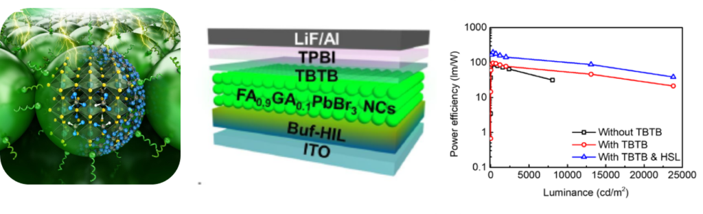
Passivated perovskite nanoparticle based LED with power efficiency > 100 lm/W.
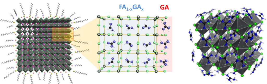
Passivation strategy for highly luminescent Perovskite Films
A large number of compositions were evaluated, allowing to identify promising low-, intermediate- and wide- bandgap perovskites with high photoluminescence quantum yield. At the edge of the perovskite crystal grain the perovskite crystal structure ends, which unavoidably leads to different chemical entities along the crystal edge. By introducing suitable cations, it is possible to ensure that all crystal edges have the same chemical structure. This process is generally referred to as passivation. In one very successful approach we developed perovskite nanoparticles that were passivated with guanidinium bromide. Once deposited in thin films these passivated nanoparticles led to a photoluminescence efficiency above 90 %.